Boolean Algebra
In working with logic relations in digital form, we need a set of
rules for symbolic manipulation which will enable us to simplify complex
expressions and solve for unknowns. Originally, Boolean algebra which was
formulated by George Boole, an English mathematician (1815-1864)
described propositions whose outcome
would be either true or
false. In computer work it is used in
addition to describe circuits whose state can be either 1 (true)
or 0 (false).Using the relations defined in the AND, OR and NOT
operation, a number of postulates are stated in Table 2.1
[Ref.3].
- P1 : X = 0 or X = 1
- P2 : 0 0 = 0
- P3 : 1 + 1 = 1
- P4 : 0 + 0 = 0
- P5 : 1 1 = 1
- P6 : 1 0 = 0 1 = 0
- P7 : 1 + 0 = 0 + 1 = 1
 Table 2.1 Boolean Postulates
Table 2.2 provides the basic Boolean theorems. Each theorem is
described by two parts that are duals of each other.
Principle of duality
1. Interchanging the OR and AND operations of the expression.
2. Interchanging the 0 and 1 elements of the expression.
3. Not changing the form of the variables.
Table 2.2 Theorems of Boolean Algebra
- T1 : Commutative Law
- (a) A + B = B + A
(b) A B = B A
- T2 : Associative Law
- (a) (A + B) + C = A + (B + C)
(b) (A B) C = A (B C)
- T3 : Distributive Law
- (a) A (B + C) = A B + A C
(b) A + (B C) = (A + B) (A + C)
- T4 : Identity Law
- (a) A + A = A
(b) A A = A
- T5 : Negation Law
- (a)

(b) 
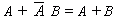
- T6 : Redundance Law
- (a) A + A B = A
(b) A (A + B) = A
- T7 :
- (a) 0 + A = A
(b) 1 A = A
(c) 1 + A = 1
(d) 0 A = 0
- T8 :
- (a)

(b) 
- T9 :
- (a)
(b) 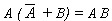
- T10 : De Morgan's Theorem
- (a)

(b) 
The theorems in Table 2.2 can be proved algebraically, by using
the truth tables or by using the Venn diagram.
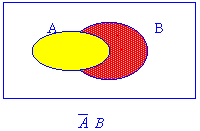
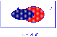
 Example 2.1 Prove T9 : (a)
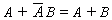
(1) Algebraically, 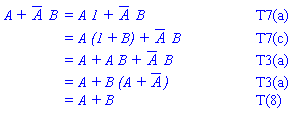
(2) Using the truth table, 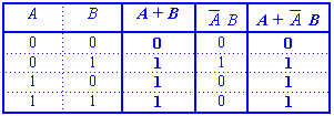
(3) Using Venn diagrams, 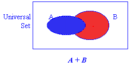
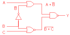
Example 2.2 Draw the circuit diagram of the Boolean expression
:
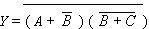
Circuit :
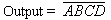
Example 2.3 Recall the definition of a NAND gate :
The output of a NAND gate is high if any of its inputs is low.
That is, the output is low only if all its inputs are
high. The Boolean expression for a 4-input NAND gate is
where Output = 0 when A = 1, B = 1, C = 1 and D = 1;
Output = 1 otherwise.
 Problem 2.1
(a) Prove T9(b).
(b) Prove T10 : (a) and (b) by completing the truth tables
below :
Click here to consult model answer.
Problem 2.2
(a) Write down the Boolean expression at the output Y of the 3-input
NAND gate,
in terms of the inputs A, B and C.
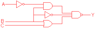
(b) Complete the truth table below for the circuit in (a).
Click here to consult model answer.
 Go to Next Chapter or
Previous Chapter or
Home Page
Go to Next Chapter or
Previous Chapter or
Home Page
 Introduction
 Basic Logic Gates