 Flip-flopsFlip-flops
 Introduction
There are several types of flip-flops : the RS F/F, the D F/F, the JK F/F and the T F/F. Among these flip-flops there are also clocked F/F and master-slave F/F. Only the simplest RS flip-flop built from NAND gates will be covered in this introductory course. The suggested applications are taken from Section 2 of the I.S.M.E.C. Electronics 13-16 Projects Manual [Ref.5]. Students must try to connect and test all the circuits in this part during their practical sessions.
 RS Flip-flop
The simplest RS flip-flop can be constructed from logic gates,
either two NAND gates or two
NOR gates.
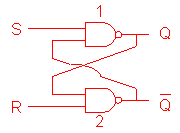
Figure 3.1 shows an RS
flip-flop wired from two NAND gates.
It has two inputs S and R
and two complementary output Q and  which are exactly opposite
to each other.
which are exactly opposite
to each other.
 |
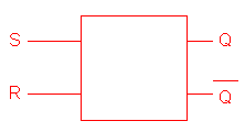 |
| (a) An RS Flip-flop | (b) Symbol |
 Example 3.1
A very special connection within the flip-flop is the
feedback
path from the output of one NAND gate into the input of other
gate. This characteristic feedback determines the truth table
of the flip-flop as well as its memory property.
For instance,
let us assume that S = 1, R = 1, Q = 0 and = 1
initially.
If S goes low, the output of NAND gate 1 goes high. Both inputs
of gate 2 are high so that = 0. This low signal is fed back to
an input of gate 1 and keeps Q = 1 even if S =1 again. For the
same reason, further change of S to 0 produce no effect.
Describe and explain what happens to the flip-flop in example 3.1 if R goes low, then high, then low and then high again. That is, two low pulses are fed to R after the flip-flop has finished the changes described in example 3.1.
 Go to Next Chapter or
Previous Chapter or
Home Page
Go to Next Chapter or
Previous Chapter or
Home Page

 Figure 3.1
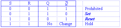
 Table 3.1: Truth Table